













Silicon Design at Every Layer
From RTL to GDSII — we design, verify, and deliver
silicon-ready ICs on AWS Cloud EDA infrastructure
- ✦ Full-Stack VLSI Design Services
- ✦ AWS Cloud EDA
- ✦ Tape-out Ready
- ✦ AI-Accelerated Design
- ✦ Devops for chip Design
Engineering the Future of Silicon Innovation
Full-Spectrum VLSI Services
From transistor-level analog to RTL verification — we handle every stage of chip design.
Analog Design
Schematic design, simulation, and optimization of analog circuits including amplifiers, PLLs, ADCs, DACs, and bandgap references.
SPICE
Cadence
Spectre
Digital Design
RTL design, synthesis, timing closure, and STA for complex digital blocks and SoC architectures at advanced nodes.
Verilog
VHDL
Synopsys
Mixed-Signal Design
Bridging analog and digital domains with co-simulation, interface design, and mixed-signal verification flows.
AMS
Virtuoso
Co-sim
Featured Projects
A selection of VLSI design engagements across process nodes and design disciplines.
Low-Power PLL for IoT SoC
Designed a fractional-N PLL targeting sub-1mW operation for a wireless IoT chip. Delivered schematic, layout, and post-layout simulation reports with full DRC/LVS sign-off.
Analog
Cadence
Spectre
High-Speed SerDes PHY
RTL design and physical implementation of a 10Gbps SerDes transceiver block. Achieved timing closure at target frequency with optimized power delivery network.
Mixed-Signal
Innovus
STA
12-bit SAR ADC
Full custom analog design of a successive approximation ADC achieving 12-bit resolution at 5MSPS. Included comparator, DAC array, and digital control logic.
Analog
SPICE
Layout
Design & Testing Labs
State-of-the-art workstations and test equipment powering every project we deliver.
Design Lab
EDA Design Workstations
High-performance Linux workstations running Cadence Virtuoso, Synopsys DC, and Innovus for schematic, layout, and synthesis workflows.
Simulation Lab
Mixed-Signal Simulation Suite
Dedicated clusters for SPICE, Spectre, and AMS co-simulation — supporting corner analysis, Monte Carlo runs, and post-layout verification.
Testing Lab
Hardware Validation & Test
Prototyping Lab
FPGA Prototyping Bench
Compute Infrastructure
EDA Compute Cluster
On-premise and cloud compute clusters for parallel simulation, formal verification, and large-scale physical design runs.
Layout Lab
Physical Design Review Station
Large-format displays for full-chip layout review, DRC/LVS debug, and floorplan analysis using Cadence Virtuoso and Mentor Calibre.
The People Behind Celvvio
Seasoned engineers with deep domain expertise across the full VLSI design stack.
ParthaSarathy
Founder & CEO
- Analog Design
- Mixed-Signal
- Cadence
- Leadership
Arun Kumar
Lead Digital Design Engineer
10+ years in RTL design, synthesis, and STA. Specializes in high-speed digital blocks and SoC integration across advanced nodes.
- Verilog
- Synopsys DC
- STA
- SoC
Sowmya Rajan
Physical Design Lead
- Innovus
- ICC2
- Calibre
- CTS
Venkat Narayanan
Verification Engineer
Builds robust UVM environments for complex IP blocks. Deep experience with constrained-random simulation and formal verification techniques.
- UVM
- SystemVerilog
- VCS
- Formal
Serving Clients Worldwide
We work across time zones to deliver silicon solutions to top semiconductor markets.
United States
Serving fabless startups and established chipmakers across Silicon Valley, Austin, and Boston.
- Silicon Valley / San Jose
- Austin, Texas
- Boston / Cambridge
- Seattle & Portland
Asia
- Bangalore & Chennai, India
- Hyderabad & Pune
- Taiwan & Singapore
- South Korea & Japan
Europe
- Germany (Munich, Dresden)
- Netherlands (Eindhoven)
- United Kingdom
- Sweden & Finland
EDA Expertise
Industry Standard Tools
Proficient in the full suite of EDA tools used across the global semiconductor industry.
Cadence Virtuoso
Synopsys Design Compiler
Cadence Innovus
Mentor Calibre
Synopsys VCS
Cadence Spectre
Xilinx Vivado
Intel Quartus
HSPICE
ModelSim / Questasim
Synopsys ICC2
Cadence Genus
Synopsys Formality
MATLAB / Simulink
Python / Tcl scripting
AI-Powered VLSI Design
RTL & Synthesis
AI-Assisted RTL Optimization
ML models predict timing violations before synthesis runs. Auto-suggest clock gating, pipeline restructuring & area reduction — cutting synthesis iterations by 40–60%.
Verification
Intelligent UVM Testbench Generation
Physical Design
ML-Driven Floorplan & Placement
Analog Design
AI-Aided Circuit Sizing
Documentation
LLM-Powered Design Docs
Signoff
Predictive Signoff Analytics
Built for Serious Silicon
We bring deep expertise and professionalism to every engagement.
IP Confidentiality
We denounce with righteous indignation & dislike men who are so beguiled to righteous demorlized.
Process Node Experience
Hands-on experience from 180nm to 7nm FinFET, across TSMC, GlobalFoundries, UMC, and Samsung foundries.
Fast Turnaround
Agile design sprints and dedicated teams ensure your milestones are met without compromise on quality.
Time Zone Coverage
Based in Chennai, India — we overlap with US, European, and Asian business hours for seamless collaboration.
Clear Communication
Weekly status reports, simulation dashboards, and always-responsive project leads — no surprises.
Cost Effective
World-class VLSI talent at competitive rates — ideal for startups and enterprises optimizing design budgets.
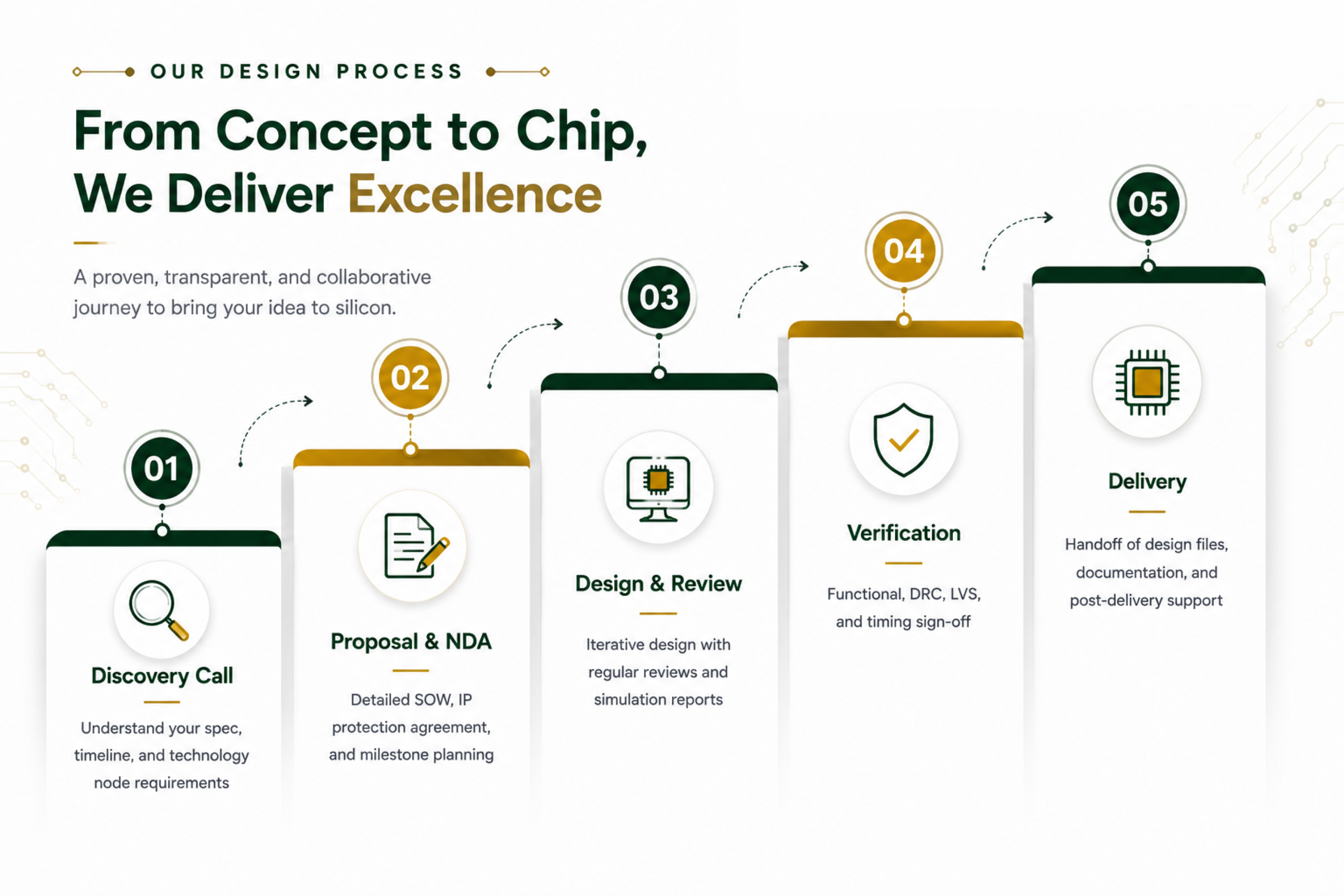
Start Your Project in 3 Simple Steps
From first contact to project kickoff in under a week
01
Send Your Requirements
Fill our design request form or email us directly
- Describe your block or design need
- Share target PDK / technology node
- Mention timeline and budget range
- Sign NDA (we provide a standard template)
Response in 1–2 business days
02
Receive Proposal & Kickoff
proposal
- Technical approach & architecture
- Fixed-price or T&M quote
- Project schedule with milestones
- Assigned engineering team intro
Proposal in 3–5 business days
03
Design Begins
- Dedicated project Slack/email channel
- Weekly progress update & milestone reports
- Simulation results & intermediate deliverables
- Final tape-out ready GDSII delivery
Kickoff same week as PO
What Our Clients Say
We build long-term partnerships grounded in technical excellence and reliability.

Celvvio delivered our PLL design ahead of schedule with exceptional simulation coverage. Their attention to corner cases and process variation was impressive.

The UVM environment they built for our DDR5 controller was production-grade. Clean code, thorough documentation, and responsive communication throughout.

We needed fast FPGA prototyping for our RISC-V core and Celvvio delivered in 3 weeks. Great team, deep skills, and competitive pricing for Asia-Pacific clients.